OUSD (R&E) critical technology area(s): Advanced Computing and Software, Microelectronics
Objective: Develop and demonstrate a prototype for photonic-electronic panel technology for the integration of photonic chips (PICs) that contain high-density three-dimensional chip-to-chip and intra-chip optical routing technology developed by the DARPA Heterogeneous Adaptively Produced Photonic Interfaces (HAPPI) program. Moving from planar to 3D optical routing is an enabling technology for PICs and when applied at the panel level enables (1) dense connectivity of multiple photonic and electrical integrated circuits and (2) a platform for seamless co-integration of optical and electrical interconnections and external interfaces.
Description: The HAPPI program is developing three-dimensional chip-to-chip and intra-chip optical routing that are compatible with standard microelectronics manufacturing processes. The program scope includes multiple routing planes within a photonic integrated circuit (PIC) or photonic interposer, connections between routing layers capable of traversing substrate thickness, and surface methods for coupling light from one photonic chip to another. This technology will enable packages that include multiple PICs with high density optical interconnects.
Notably outside of the HAPPI program scope is waveguide-to-fiber coupling and larger scale chip-to-chip connectivity at the system board level. A commercial opportunity exists to create a platform similar to an electrical printed circuit board (PCB) platform that incorporates 3-dimensional optical routing planes, co-integration of optical and electrical routing, interconnections to photonic and electronic integrated circuits and an interface with fiber arrays for long-reach signaling.
This SBIR will develop photonic-electronic panels for multi-chip integration capability as a manufacturable, commercially available, low-cost technology. Solutions developed under this topic should meet a within panel optical interconnect pitch of 100-300 um that show non-blocking routing as well as co-integration with electronic wiring. A >16 channel detachable fiber attach unit (FAU) should be developed as a method to introduce photonic signals to the panel. A minimum of two integrated circuits (ICs) must be mounted to the panels that integrate with the embedded signaling pathways. This mounting scheme could employ flip chip bonding IC, optical bumps, or other equivalent surface mount like bonding technologies. A minimum of two IC components should be chosen such that they can demonstrate the ability to route both optical and electronic signals and are available commercially or from a foundry. The finalized integration of FAU, panel, and ICs is expected to meet the point-to-point optical link budget as specified in Table 1 below. In addition to meeting the link requirements for insertion loss (terminating at the PIC) the designed routing must demonstrate built-in optical loopback, e.g. a continuous optical loop from insertion point at the FAU through the system, in and out of a PIC, and returning to back to the same FAU. A notional schematic is included in Figure 1 to provide a visualization of the panel concept, the required loopback path, and highlight the two optical interfaces (OI-1 and OI-2) and waveguide (WG) components of the link budget. The panel prototype units delivered at the end of Phase II must be self-contained, environmentally robust, and meet minimum performance metrics.
Table 1. Phase II Metrics
| Metric | Target |
|---|---|
| Panel size1 | Scalable to > 300 x 300 mm |
| Interconnect pitch | 100-300 µm |
| Multilayer panel routing | Demonstrate non-blocking routing and co-integration with electrical routing |
| Fiber attach unit (FAU) | Detachable, ≥ 16 fiber array |
| Link loss 2 | Total insertion loss ≤ 2 dB) |
| Mounted components | > 2 ICs 3 |
1 50 x 50 mm demonstrated with experimental evidence for technology scalability to >300 x 300 mm.
2 Link loss includes (1) OL-1: connection between PIC and panel (< 0.5 dB), (2) WG: routing within the panel and connection (< 3dB/m), (3) OL-2 between panel and FAU definition (<0.5 dB) (see Figure 1 for illustration)
3 Two or more foundry fabricated or commercially available ICs that when combined demonstrate both photonic and electronic connections to the panel.
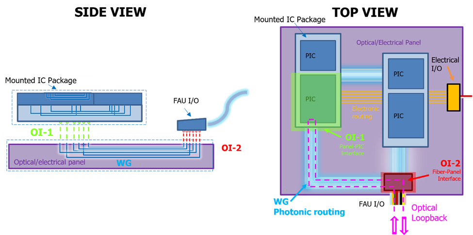
Figure 1. Side View and Top View of notional panel systems, highlighting main components and photonic interfaces specified in the program metrics.
Phase I
Phase I will focus on demonstrating the feasibility of the panel architecture and a fabrication plan. An appropriate material platform and method for integrating optical and electrical routing in a large sized panel should be determined along with a concept for the external fiber connector coupling to the panel. A strategy for IC attach and coupling to the panel’s photonic-electronic routing should be developed. Designs must provide detailed modeling and simulation to show the achievable link budgets for the method of coupling at the various interfaces, supported by experimental data from small-scale testing of individual components links or from prior work. At the end of Phase I, the Performers should provide a report which includes: detailed description of the design including simulation and experimental results, fabrication plan for the design, description of electronic and photonic IC components (minimum 2 ICs) to be integrated, and a test plan for assessing the realized panel performance.
Schedule/Milestones/Deliverables:
- Month 1: Report on initial panel material platform, IC attach concept, and external fiber uplink
- Month 6: Interim report demonstrating simulated/small scale testing of link losses in panel routing, panel to IC coupling, and FAU mount
- Month 8: Final Phase I Report summarizing approach in preparation for Phase II; detailed description of design, fabrication plan, description of electronic and photonic IC components to be integrated, and a test plan.
Phase II
Phase II will cover the fabrication of the Phase I designs that demonstrate a detachable fiber array unit connection to a panel board that fans out into multilayer routing and couples to on board IC components. Realized designs should incorporate two ICs that demonstrate the ability to route both photonic and electronic signals on the same panel platform. In addition to meeting the link loss requirements specified, the panel prototype should include at least one photonic link with continuous loopback. A packaging compatibility report should be included to outline the methods and constraints for bonding/coupling the chosen ICs to their panel systems. As Phase II is focused on fabrication and assembly, milestones include interim reports on individual components and links as the project proceeds toward final system assembly. By the end of Phase II, the Performers must deliver ten panel prototype units meeting the program metrics and a Final Program Report detailing the fabrication process and characterization data for delivered prototypes*.
* All prototypes should be provided with adequate instructions to support government testing and evaluation using standard laboratory equipment.
Schedule/Milestones/Deliverables
- Kickoff: System Requirements Review (SRR), to include risk analysis
- Month 3: Documented completion of finalized panel design and component layouts; IC selection and sourcing. Report on fabrication and assembly schedule.
- Month 6: Market Study Report on application requirements, potential customers, and commercialization strategy.
- Month 9: Interface Compatibility Report describing the IC to panel interface design and assembly including compatibility requirements and design constraints
- Month 12: Report describing photonic-electronic panel post fabrication results, and assembly plan for IC attach and FAU I/O.
- Month 18: Demonstration of photonic-electronic panels meeting program metrics; Final Report for Phase II Period to include characterization data for the link loss.
Phase III dual use applications
Phase III work is typically oriented towards commercialization of SBIR/STTR research or technology with funding obtained from either the private sector, a non-SBIR/STTR Government source, or both, to develop the technology into a viable product for sale in military or private sector markets. It is envisioned that the technology developed under the SBIR program will have dual-use commercial and Department of War (DOW) applications. In the commercial space, the vision is for these panel sized interposers to enable interconnectivity of PICs with broader external systems. Optical interfaces between components are expected to be key enablers in this area as the ability to move signal in and out of the microsystem efficiently is critical. In the DOW domain, the optical panel platforms are anticipated to be a key building block for high-performance co-packaged optical systems for photonic computing, signal processing, sensor arrays, and high bandwidth communication modules.
References
Keywords
Photonic, Advanced Microsystem Packaging, Optical Packaging, Optical Fiber Attach, Photonic Integrated Circuits, Optoelectronics
TPOC-1-PoC
DARPA BAA Help Desk
This program is now complete
This content is available for reference purposes. This page is no longer maintained.
Opportunity
DPA26BZ01-NV002
Closed: June 3, 2026
Solicitation
DoW SBIR 2026 BAA