Published June 2020
Developing a breakthrough microprocessor
Combining many of the best traits of photons and electrons on a single silicon chip
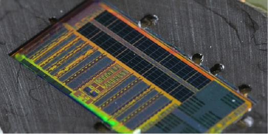
This electronic-photonic processor integrates on a single chip more than 70 million transistors and 850 photonic components that provide logic, memory, and interconnect functions. It was developed with support from several DARPA programs, among them the Photonically Optimized Embedded Microprocessors (POEM) program.
Source: DARPA
Need and Opportunity
Since the 1970s, DARPA has been a champion of progress in microelectronics technologies. The agency’s research and development efforts helped enable nearly a half-century of exponential growth in the number of transistors on computer chips and a staggering increase in processing power. While chip performance has increased dramatically, the rate at which data can move between chips and other electronic components has lagged.
This problem is especially acute in modern applications, such as machine learning and high-speed communication, which require massive data movement between processors and memory. In recent decades, DARPA recognized that enlisting photons instead of, or in tandem with, electrons in the operation of microprocessors could help speed up the transfer of data between chips on the same or different circuit boards. Although electrons have been the fundamental embodiments of ones and zeroes in integrated circuits (ICs), photons could serve as fast-as-light carriers of information between chips, overcoming digital traffic jams that put the brakes on electrons.
Historically, photonic integrated circuits (PICs) had been fabricated on expensive “exotic” materials like gallium arsenide (GaAs), limiting their use to niche applications. That began to change in the early 2000s with the widespread availability of silicon-on-insulator (SOI) wafers for microprocessors, which enabled photonic waveguides on silicon. SOI wafers opened a way for engineers to accelerate PIC development by leveraging the existing manufacturing infrastructure established by the electronics industry. Even more critically, photonic devices based in silicon would enable co-integration with advanced electronics, providing a way of seamlessly interconnecting electronics and photonics.
Although constructing basic waveguides in silicon was a significant leap forward early in the new millennium, many of the active and passive components of photonic systems – lasers, modulators, photodetectors, and couplers, for example – had not yet been demonstrated on a silicon platform. Without these key components for generating and manipulating laser light in microsystems, the use and impact of the technology would be limited.
DARPA Solution
In 2005, DARPA began the Electronic & Photonic Integrated Circuit (EPIC) program to develop technology for fabricating high-performance photonic circuits on a silicon chip within the industry’s most prevalent manufacturing framework known as CMOS (complementary metaloxide semiconductor). The goal of EPIC was to develop a breakthrough microprocessor that combined many of the best traits of photons and electrons on a single silicon chip.
Much like DARPA’s earlier investment in the fundamental science and engineering underlying microelectronics, silicon photonics had the potential to enable photonics systems with unprecedented performance and functionality across a broad range of applications. The program’s research teams largely came from academic institutions, including the Massachusetts Institute of Technology (MIT); University of California, Los Angeles (UCLA); University of California, Santa Barbara (UCSB); and the California Institute of Technology. The researchers developed passive components, fabrication techniques, and device designs needed to create PIC technology.
The team led by MIT designed and demonstrated a number of key photonic components. One of these was a germanium-based photodetector, which was fabricated on silicon where it would be critical to the key function of measuring light directly on-chip. For its part, the UCSB team demonstrated a groundbreaking hybrid silicon laser, enabling the generation of light on silicon. Since silicon doesn’t intrinsically support on-chip generation of light, this was a significant feat of engineering. The components developed by MIT and UCSB were key to generating and receiving light onchip, which is essential to powering photonic data movement. In parallel with EPIC, DARPA led the University Photonics Research Centers program – a fundamental research initiative that funded 50 individual projects across various universities. Each project focused on advancing the scientific understanding of semiconductor optical physics, revealed knowledge gaps, and identified areas worthy of future investment.
The EPIC program culminated with the first complete integration of all photonic components required to create a silicon photonic circuit. With this suite of components now available, designers have been able to build custom optical systems tailored to their unique application needs. These accomplishments have had a pervasive impact across the Department of Defense (DOD).
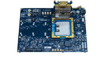
This field programmable gate array (FPGA) board developed by Intel and Ayar Labs replaces some electronic input/output interfaces with optical interfaces.
Source: Courtesy of Ayer Labs
Impact
The successful development and proof of feasibility of a silicon photonics platform under the EPIC program has enabled a host of defense applications. These include advanced positioning, navigation, and timing (PNT) technology; autonomous navigation; long-range 3-D mapping; and highspeed communications. Because these contributions are grounded in the manufacturing processes and equipment long employed by the microelectronics industry, they catalyzed the commercialization of silicon photonics.
This novel category of technology has been readily adopted by universities, commercial companies, DOD, and foundry service providers that can manufacture microsystems to circuit designers’ specifications. Further, the manufacturing ecosystem spawned by EPIC has streamlined the rapid prototyping of innovative photonic circuit concepts. While several countries are only recently beginning to invest in their foundry and integration capabilities, DARPA’s early funding in fundamental research related to silicon photonics has allowed the U.S. to commercialize and maintain a global technological lead in photonics to this day. EPIC’s R&D accomplishments also spawned new DARPA programs — including the Electronic-Photonic Heterogeneous Integration (E-PHI) and Photonically Optimized Embedded Microprocessors (POEM) programs — to open the way to yet more sophisticated silicon photonics technology.
The hybrid silicon laser developed by the EPIC team at UCSB became a critical piece of Intel’s silicon photonics products. And Ayar Labs, a start-up that spun out of the POEM program, is working with Intel and Global Foundries to develop high-bandwidth optical communications products for applications that include high performance computing and artificial intelligence.
Looking Ahead
EPIC’s research has also parlayed into advanced router technology. Following the program’s conclusion, one of the commercial performers – Luxtera – was acquired by Cisco to support its router business. Similarly, the DARPA E-PHI program funded the optoelectronics firm Aurrion, Inc., which was later acquired by Juniper Networks to support its router products.
Between these two acquisitions, EPIC has directly influenced over 70% of the worldwide router market share. Revenue from silicon photonics products is expected to grow to over $1 billion in 2020, led by Intel and Cisco. Meanwhile, the legacy of the EPIC program continues to expand at DARPA, most recently in the launch in 2019 of agency’s Lasers for Universal Microscale Optical Systems (LUMOS) program.
You might also like

Stealth systems enhance defense
Advanced technologies reduce detection and improve survivability across multi-domain operations worldwide. | Learn more

Mosaic warfare drives flexibility
Modular systems work together to create adaptable, quick-response forces for today's complex battles. | Learn more

ARPANET, the internet's genesis
Packet-switching networks enabled resilient, distributed information sharing that transformed worldwide digital connectivity. | Learn more
Quantum sensing and computing
Establishing defense capabilities through ultra-precise sensing and revolutionary computational breakthroughs. | Learn more